Mohit R Khurana

Mohit R Khurana

Semiconductor Advanced Packaging • Heterogenous Integration • Advanced Packaging Architecture

🔬 8+ Years Materials Science Experience 💻 6+ Years Advanced Packaging Experience 🏆 Semicon West 20 Under 30 Awardee ✅ Led Pathfinding, Development & Qualification

Biography

I am a semiconductor packaging leader specializing in advanced packaging and substrate technologies and advanced packaging architectures that enable next-generation CPUs, GPUs, and AI accelerators.

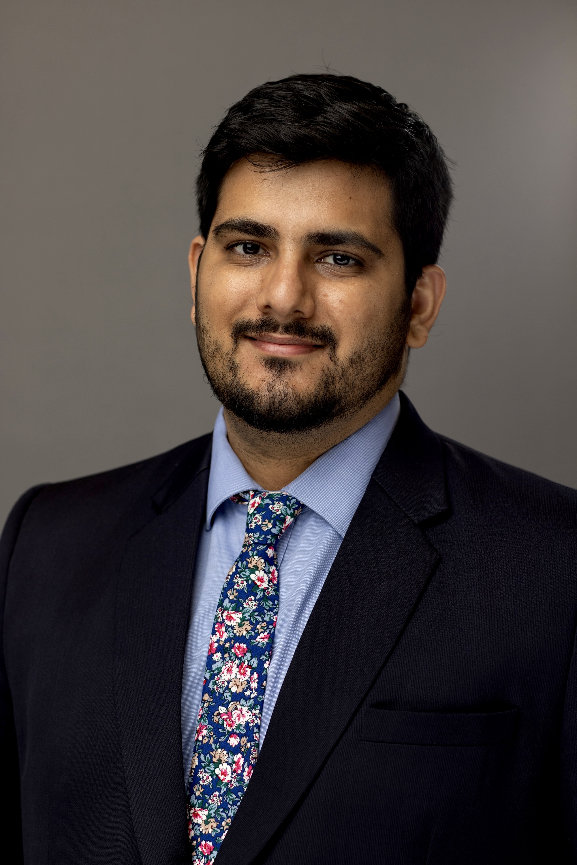
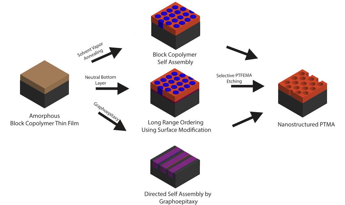
I’m a materials scientist and polymer technologist from Mumbai, India, currently living in Chandler, Arizona. I earned my bachelor’s degree in Polymer Engineering, focusing on polymer blending and structure–property relationships. My curiosity about applying polymers to the broader field of materials science led me to pursue a master’s in Materials Science at Cornell University, where I worked on block copolymer self-assembly of stable radical polymer blends. During my master’s, an internship at Intel introduced me to advanced semiconductor packaging, a field that quickly became my niche.

At Intel, I have directed cross-functional teams spanning materials, design, and manufacturing to deliver substrate and package solutions that directly impact multi-billion-dollar product platforms. My work extends beyond execution: I influence technology roadmaps, evaluate ecosystem readiness, and ensure scalability from pathfinding through high-volume manufacturing.

Recently, I’ve led package architecture definition and developing technology strategies to align with Intel Foundry’s roadmap for 2.5D, 3D, and 3.5D architectures. In the past, I led pathfinding of key materials technologies that enabled Intel’s AI GPU packaging, including large form factor stiffener technology and EMIB-T materials technology. I’ve also pioneered new approaches, developing first-of-their-kind characterization techniques using AFM and XRD for advanced packaging. My work has resulted in 8 external publications and 7 internal publications in Intel’s packaging technology journal.

Recognized as an emerging industry leader by SEMI Americas' Semicon West 20 under 30, I actively contribute to the semiconductor packaging community through publications, peer-review, and cross-industry collaborations. My leadership philosophy combines technical depth with vision, enabling packaging strategies that accelerate the compute scaling while balancing cost, manufacturability, and performance.

Experience

April 2025 — Present
Sr. Packaging Architect
Adv Design & Customer Enabling, Advanced Packaging & Technology Manufacturing
Intel Foundry, Intel Corporation
  • Impact: Responsible to manage Intel Foundry's packaging roadmap and offerings to customers, across Intel's global factories and customer base. Recommendations to management result in new pathfinding programs and disposition of existing programs to capability offerings.
  • Determine and recommend the roadmap strategy for key interconnect and technology building blocks (HSIO, power delivery, thermals, etc) through analyzing customer demand, market trends and competitive intelligence. Developed and recommended pathfinding strategy for EMIB-T and and RDL interposer architectures to enable a competitive roadmap.
  • Perform trade-off analysis for multiple package scenarios (layout, substrate technologies, thermals, etc) to determine recommendation for TV strategy, for meeting customer demand and ensuring a competitive foundry roadmap.
  • Summarize and present market trends and competitive analysis to ensure a competitive foundry roadmap.
October 2021 — April 2025
Sr. Packaging Engineer
Materials Technology Development, Advanced Packaging & Technology Manufacturing
Intel Foundry, Intel Corporation
  • Impact: Selected and completed technology maturity for materials used in the 1st gen EMIB-T architecture, which enables heterogenous integration for extremely large form-factor and die complexes used in AI packages. Completed pathfinding of stiffener technology used in large form factor AI packaging meeting SMT yield and overall reliability targets.
  • Led pathfinding and selection of EMIB-T materials through a cross-platform team of over 8 engineers, demonstrating successful test vehicle data.
  • Led stiffener and adhesive materials pathfinding for large form factor packages, through a cross-platform team of 6 engineers and roadmap-ed the technology for the foundry roadmap. Published in Intel’s packaging journal.
  • Successfully qualified thermal materials and process through IHS and TIM optimization for lid attach process.
  • Successfully qualified packaging materials and managed materials program for Intel® Core™ (12th and 13th Gen), Agilex™ FPGAs, and drove successful pathfinding of Intel's AI GPU packages.
August 2019 — October 2021
Packaging Engineer
Yield, Advanced Packaging & Technology Manufacturing
Intel Foundry, Intel Corporation
  • Impact: Developed first-of kind AFM and XRD technologies for advanced packaging. Selected and procured $1M+ tools and hired 10+ head-count to grow the lab tool capabilities.
  • Drove characterization efforts leading to build-up technology selection for EMIB substrate manufacturing enabling HSIO specs for Intel® Xeon® (4th and 5th Gen) data center CPUs.
  • Characterized organic adhesive film leading to development of a low loss substrate build-up solution for data center applications. Elucidate structure-property relationship aimed at improving dielectric-copper adhesion. Published as an IEEE ECTC 2022 proceedings.
  • Led lab characterization tools capability expansion through first-of-a kind tool capability development and procurement with tool suppliers.
  • Demonstrated innovation though novel industry leading technique development using AFM, XRD and SEM techniques. Published 2 papers in Intel’s packaging journal and an external paper in Materialia.
  • Interviewed and recruited over 10 engineers and technicians resulting in team expansion.

Education

2017-2019
Cornell University
Degree: M.S. in Materials Science & Engineering
GPA: 4.02/4.00
  • Thesis: Nanostructured Stable Radical Polymer Thin Films: A Battery Electrode Material.
  • Motivation: Stable radical polymers can be leveraged as an inexpensive electrode material due to their fast redox reactions, enabled by the free radical moiety on the side chain. However, they suffer from low conductivity due to the inherent insulation properties of the polymer backbone. Electron hopping of the stable radical from one side chain to another can potentially enable higher conductivity. This work used copolymerization to control the spacing between stable radical side group domains in a precise manner, to study and enable electron hopping. A fluorinated copolymer was used due to its ability to phase separate with ease, allowing precise domain control.
  • mastersthesis
  • Key Challenges: Phase separation and self assembly in precise domains; characterization of the nano-domains; development of nano-structures enabling higher electrolyte porosity.
  • Accomplishments: Optimized directed self assembly through solvent vapor and thermal annealing resulting in lamellar and cylindrical; Optimized underlayer and graphoepitaxy resulting in long range order in both lamellar and cylindrical domains; Characterized thin film structure through AFM and SEM; Developed nano-structured cross-linked polymers for improved surface area of active sites.
  • Publication: Block copolymers containing stable radical and fluorinated blocks with long-range ordered morphologies prepared by anionic polymerization.
  • Poster: Nanostructured Stable Radical Block Copolymers for Next Generation Batteries.

cornell logo

2013-2017
Institute of Chemical Technology
Degree: B.Tech. in Polymer Engineering
GPA: 8.82/10.00
  • Thesis: High Impact Resistant Polyolefin Blends for Houseware Applications.
  • Motivation: Polyolefins are commonly used in houseware and bottle applications. However, they suffer from low impact and tear resistance limiting their load bearing capability. This can be improved using copolymerization, chemical modification or blending with higher impact resistant materials. In this work, polymer blending was leveraged, considering it is an easier and cost effect method to modify properties. Homopolymer and random copolymer polypropylene was used as the base polymer while poly(ethylene-co-octene) and styrene-butadiene-styrene rubber were used as additives to improve properties.
  • stressvstrain

  • Key Challenges: Determining appropriate blending material to meet performance targets; optimizing blend phase separation through concentration, material type and process experiments; compatibliizing blends to avoid structural defects; developing a blow-molding compatible blend for bottle application.
  • Accomplishments: Determined target materials specification using maket and industry survey of houseware products; studied blend using 2 elastomer systems for mechanical and viscoelastic properties; improved properties using a compatibilizer additive; determined an optimized blend composition with 8x impact resistance and 3x elongation before break compared to the unblended polypropylene, without significantly reducing tensile strength.

  1. A. Cintora, H. Takano, M. Khurana, A. Chandra, T. Hayakawa, C. Ober, “Block copolymers containing stable radical and fluorinated blocks with long-range ordered morphologies prepared by anionic polymerization,” Polymer Chemistry 10, 5094, (2019). link🔗
  2. Mohit R. Khurana, Alicia Cintora, Christopher Ober, “Directed Self Assembly of a Stable Radical Polymer” 2018-2019 Research Accomplishments CNF, page 200, 2019. link🔗
  3. N. Badwe, P. Daharwal, T. Rawlings, P. Diglio, S. Wozny, M. Khurana, P. Tadayon, G. Hsieh, M. Renavikar, “High-temperature mechanical properties and fatigue of nanocrystalline nickel-cobalt-phosphorous (NiCoP) alloy,” Materialia. 18, 2589, (2021). link🔗
  4. Y. Yang, M. Wall, R. Shanmugam, S. Wozny, X. Yan, M. Khurana, R. Ranjan, D. Seneviratne, K. Nikkhah, S. Nad, “Characterizations and Challenges of Adhesion Promotion Solutions for HSIO Package Development”, 2022 IEEE 72nd Electronic Components and Technology Conference (ECTC), San Diego, CA, USA. 648, (2022). link🔗
  5. M. Ayalasomayajula, M. Ravi Khurana, V. Balakrishnan, P. Shiva Chaudhary, S. Basu Bal and R. Kumar Baranwal, “Advancements in Wearable Solar Cell Technology: Integrating Perovskites and Dye-Sensitized Cells,” IEEE Journal on Flexible Electronics, vol. 3, no. 5, (2024). link🔗
  6. M. Khurana, M. Ayalasomayajula, P. S. Chaudhary “Selective Atomic Layer Etching for Silicon Device Fabrication,” IEEE ICIC3S, Una, India, (2024). link🔗
  7. M. Ayalasomayajula, M. Khurana, P. S. Chaudhary "Effects of process parameters on Ga2O3 fabricated by MBE, HVPE and MOCVD" IEEE ICIC3S, Una, India, (2024). link🔗
  8. M. Ayalasomayajula, M. Ravi Khurana, P. S. Chaudhary, “Electrically Conductive Adhesives in Microelectronics Packaging,” ASME. J. Electron. Packag, 1-8, (2024). link🔗

SME 30 Under 30 🏆

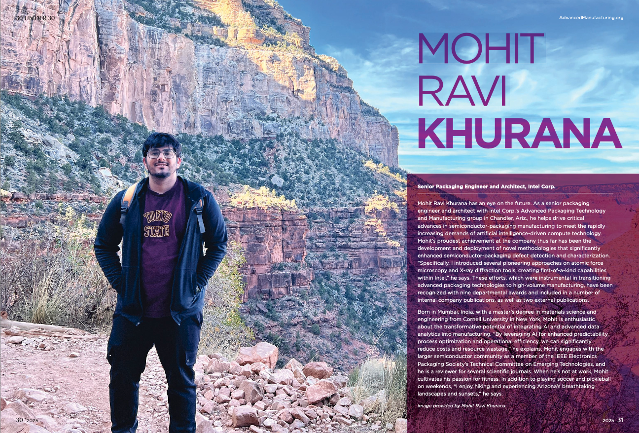
Year: 2025

Awarded by SME

SME spotlights the significant talent, contributions and innovation of young people impacting the future of manufacturing.

award

Semicon West 20 Under 30 🏆

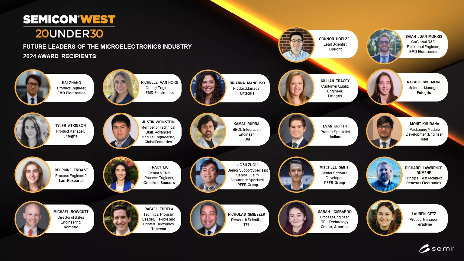
Year: 2024

Awarded by SEMI Americas

For demonstrating outstanding leadership, practicing productive collaboration, exhibiting commitment to success and actively engaging in the community.

award

Member of the Royal Society of Chemistry 🏛️

Elected Member since 2025.

About the organization: UK’s professional body for chemical scientists with a worldwide community.

Organization Website 🔗

Member of the IEEE EPS Technical Committee on Emerging Technologies 🏛️

Committee Member since 2023.

About the committee: Focuses on emerging, novel and unique material and packaging solutions. This committee places an international focus on the development, characterization, and commercial support for packaging, assembly, and test infrastructure for key applications areas such as, Fluidic Systems, Optical Systems, Automotive Systems, Military Systems, Medical Systems, Remotely Operated Systems, Telecommunications.

Committee Website 🔗

Research Interests

  • Advanced packaging architectures: Novel architectures that scale to larger die complexes, higher bandwidths, higher thermally designed power and efficient system-level i/o.
  • Advanced packaging interconnects: Development of reliable high density silicon interposer interconnects, silicon bridge interconnects, hybrid bonded interconnects, and optical interconnects.
  • Substrate technology: Development of substrate core technology, build-up technology, bump pitch scaling, power delivery and HSIO for large multi-die packages.
  • Warpage control and stress mitigation for AI GPUs and large form-factor packages through on and within package technologies like stiffener and substrate core.
  • Novel packaging materials for wafer and package assembly.
  • Advanced packaging characterization and defect detection.

Benefits and Drivers for Advanced Packaging

  • Enables heterogeneous integration of chiplets and components on the same package. Examples: HBM memory, compute and graphics processing units on the same package.
  • Enables disaggregation of chiplets into smaller sizes to improve yield resilience.
  • Enables customization of die-die interconnections with benefits such as leveraging different and custom IPs on the same package, use of different i/o densities at different interfaces, etc.
  • Enables improved off-package communication on the system level to improve system performance.
  • Enables advanced thermal solutions on the package and system level, to keep up with the growing thermal demands with compute scaling.
  • Enables high speed I/O and power delivery solutions to meet growing data rate, thermally defined power requirements.

What is a Semiconductor Package?

Why is Packaging Needed?

Standard vs Advanced Packaging